Are your expensive solder pallets degrading far faster than you expected? This premature wear and tear isn’t just a budget issue; it’s a direct threat to your production quality, causing defects and costly line stoppages.
To maximize the lifespan of solder pallets, you must adopt a holistic strategy: implement rigorous and regular cleaning with appropriate solvents, use correct horizontal storage to prevent warping, enforce careful handling protocols, optimize soldering thermal profiles to reduce material stress, and establish a proactive inspection and maintenance schedule.

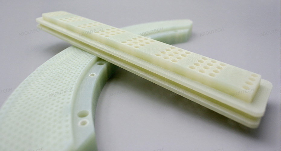
I’ll never forget the frustration from early in my manufacturing career when we invested in a new set of high-grade composite pallets for a lead-free line. We expected them to last for years, but within months, we started seeing signs of warping and surface degradation. The result was a sudden spike in soldering defects that sent our quality team scrambling. It was a painful lesson: these pallets are not just simple holders; they are precision instruments critical to the entire process. It was only when we started treating them with the respect they deserved that we saw a dramatic improvement in both their longevity and our product yield. This guide shares the exact five strategies we implemented to turn things around.
Why is Meticulous Cleaning the First Line of Defense for Pallet Longevity?
Think cleaning your pallets is just about appearances? The residue left behind after soldering is a silent killer, slowly eating away at your investment and compromising your process.
Regular, proper cleaning is non-negotiable because it removes corrosive flux residues that chemically attack the pallet material. This prevents surface degradation, maintains dimensional accuracy, and ensures consistent thermal performance, directly impacting soldering quality and pallet lifespan.

Dive Deeper: The Science Behind the Cleanliness
The importance of cleaning goes far beyond simple housekeeping. It’s a fundamental process control activity that directly impacts the reliability of your final product. After each pass through the wave solder machine, the pallet is coated with a cocktail of residues, the most damaging of which is the soldering flux. While essential for the soldering process, most fluxes contain activators that are acidic and corrosive by nature. When left on the pallet surface, these chemicals begin a slow but relentless attack on the composite’s resin matrix. This chemical erosion leads to surface pitting, which makes the pallet harder to clean in the future and creates sites where solder balls can become trapped, potentially transferring to the next Printed Circuit Board Assembly (PCBA).
Furthermore, baked-on flux residue acts as an insulator. This can cause uneven heating across the pallet surface during subsequent cycles. The resulting differential in thermal expansion can introduce micro-stresses into the material, contributing to gradual warping over time. A warped pallet cannot hold the Printed Circuit Board (PCB) perfectly flat, which is a recipe for disaster in modern electronics manufacturing, leading to classic soldering defects like open circuits (non-wetted leads) and solder bridging (shorts). For assemblies with fine-pitch Surface Mount Technology (SMT) components or sensitive Ball Grid Arrays (BGAs), maintaining planarity is absolutely critical. A clean pallet is a predictable pallet, and process predictability is the cornerstone of achieving a high Process Capability Index (Cpk).
| Cleaning Action | Rationale | Consequence of Neglect |
|---|---|---|
| Use Approved Solvents | Prevents chemical damage to the composite resin. | Harsh solvents can cause swelling, softening, or delamination. |
| Clean After Every Shift | Removes corrosive flux before it can cause damage. | Permanent surface pitting and material degradation. |
| Use Soft Brushes/Cloths | Avoids scratching the pallet’s smooth surface. | Scratches trap contaminants and become stress points for cracks. |
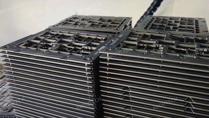
How Does Improper Storage Silently Destroy Your Pallet’s Integrity?
You’ve finished a production run and stacked the pallets in a corner. What’s the harm? This common practice is one of the leading causes of premature pallet failure through a slow, invisible process.
Improper storage, especially vertical stacking or placement on uneven surfaces, allows gravity and mechanical stress to cause gradual material creep and warping. This permanently compromises the pallet’s flatness, leading to inconsistent soldering and a drastically reduced useful life.

Dive Deeper: The Physics of Pallet Deformation
High-performance composite materials are incredibly rigid, but they are not immune to the laws of physics. When a pallet is stored improperly—leaned against a wall, stacked unevenly, or placed on a non-flat surface—it is subjected to continuous, localized stress. Over time, this sustained load causes a phenomenon known as "creep," which is the tendency of a solid material to move slowly or deform permanently under the influence of persistent mechanical stresses. For a solder pallet, this deformation manifests as warping, bowing, or twisting.
Even a warp of just 0.5mm, barely visible to the naked eye, can be catastrophic for the wave soldering process. A warped pallet means the PCB it holds is no longer perfectly parallel to the surface of the molten solder wave. As the board passes through the process, some areas will be too close to the wave, leading to excessive solder pickup, bridging, and shorts. Other areas will be too far away, resulting in insufficient solder, skips, and open joints. This inconsistency makes achieving a stable, repeatable process impossible and directly degrades the quality and reliability of the final PCBA. The worst part is that this damage is often irreversible. Once a pallet has warped, it cannot be reliably flattened, and its use will continue to generate defects. Proper storage is not an optional best practice; it is a mandatory requirement for protecting your investment and ensuring process control.
| Storage Method | Why It’s Critical | The Risk of Doing It Wrong |
|---|---|---|
| Store Horizontally | Distributes the pallet’s weight evenly. | Leaning or vertical storage creates stress points that lead to bowing. |
| Use Flat, Level Shelving | Provides uniform support across the entire pallet. | Uneven surfaces transfer their shape to the pallet over time. |
| Avoid Random Stacking | Prevents localized pressure from damaging features. | Stacking can damage hold-downs, masking edges, and the pallet surface. |
Is Careless Handling the Most Preventable Cause of Pallet Failure?
A dropped pallet, a chipped corner—these might seem like minor incidents in a busy factory. In reality, every physical impact is a significant blow to the pallet’s precision and lifespan.
Yes, careless handling is a primary and entirely preventable cause of pallet failure. Physical shocks from drops or collisions cause chips and micro-cracks that compromise critical masking features and can propagate into major fractures under thermal stress, ruining the pallet.

Dive Deeper: From Micro-Cracks to Macro-Failures
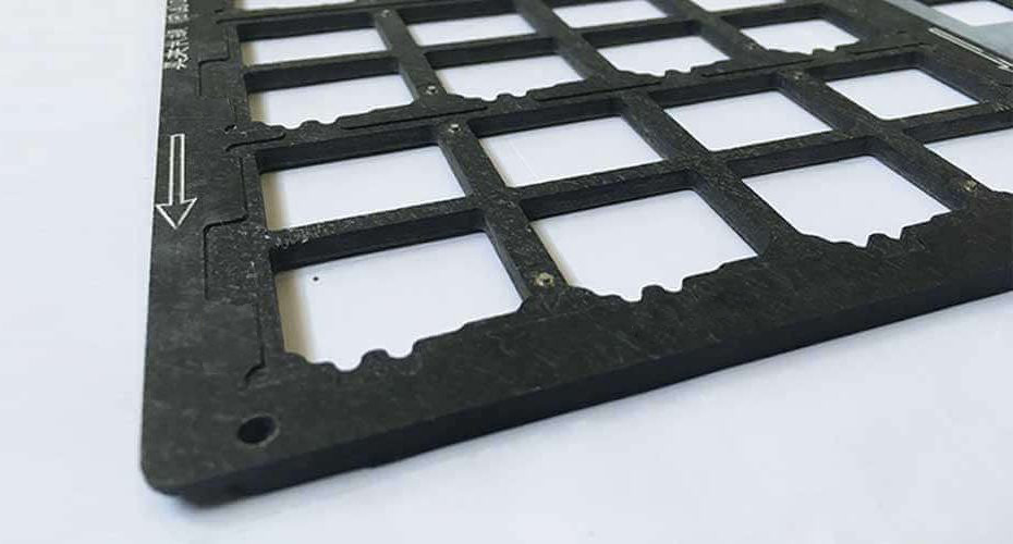
While thermal and chemical stresses are gradual, physical impact delivers an acute, often fatal, blow. A solder pallet is a piece of precision tooling, and its value lies in its dimensional accuracy. A chip on the edge of a pocket designed to mask a BGA can allow molten solder to wick underneath, destroying the component. A dent on a locating feature can cause the PCB to be misaligned, shifting the entire soldering pattern.
The most insidious damage, however, comes from micro-cracks. A pallet that is dropped or knocked against a hard surface may look fine initially, but the impact can create tiny fractures within the material matrix. When the pallet is then subjected to the extreme thermal shock of the soldering process—going from room temperature to over 260°C and back again—these micro-cracks become stress concentration points. With each thermal cycle, the cracks grow slightly larger, a process known as thermal fatigue. Eventually, what started as an invisible flaw propagates into a full-blown solder crack or fracture, rendering the pallet useless.
This is why establishing and enforcing strict handling protocols is not micromanagement; it’s essential asset protection. Implementing Standard Operating Procedures (SOPs) for transporting, loading, and unloading pallets, and training operators on their value, can eliminate the vast majority of these failures. A damaged pallet introduces random, unpredictable defects into your process, making any form of systematic problem analysis or troubleshooting incredibly difficult. Protecting pallets from physical harm is one of the easiest and most effective ways to maintain process stability.
Can Optimizing Your Solder Process Actually Save Your Pallets?
Your soldering process is designed to create perfect solder joints on the PCBA. But could that same process be unintentionally destroying the tool that makes it possible?
Absolutely. Optimizing your soldering process, specifically the thermal profile, is crucial for pallet preservation. By minimizing peak temperatures and dwell times to the lowest effective levels, you reduce the cumulative thermal stress on the pallet material, significantly slowing material aging and extending its life.

Dive Deeper: The Cumulative Effect of Thermal Stress
The composite materials used for solder pallets are engineered for high-temperature environments, but they are not invincible. Every single thermal cycle—the journey through the pre-heat zones and the solder wave—contributes to the material’s aging process. This aging manifests as a gradual loss of mechanical strength and an increase in brittleness. While you cannot eliminate thermal cycles, you can control their intensity and duration.
This is where the optimization of your thermal profile becomes critical. In SMT assembly, this is often called the reflow profile. The goal is to achieve perfect solder wetting and joint formation with the minimum amount of thermal energy necessary. Running the process hotter or longer than required "just to be safe" is a common but destructive practice. That extra heat doesn’t just stress the electronic components; it dramatically accelerates the degradation of the pallet material.
A well-designed wave solder process involves carefully profiling the PCBA within the pallet to find the optimal balance. This means ensuring the solder joints reach the correct temperature for the right amount of time, while keeping the pallet’s overall exposure as low as possible. This is a core principle of Statistical Process Control (SPC): understanding your process window and operating consistently within it. By investing time in process optimization, you create a win-win scenario: you improve the quality and reliability of your solder joints while simultaneously extending the life of your most critical tooling.
Why is a Proactive Inspection Plan Your Ultimate Longevity Strategy?
Waiting for a pallet to fail on the production line is the most expensive maintenance strategy. How can you get ahead of failures before they cause a crisis?
A proactive inspection plan is the ultimate strategy because it shifts you from reactive repair to preventative maintenance. By regularly checking for wear, damage, and warping, you can identify and address minor issues before they escalate into catastrophic failures that cause production downtime and quality escapes.
Dive Deeper: Maintenance as a Quality Management Tool
The most advanced manufacturing operations treat maintenance not as a chore, but as a form of data collection for continuous improvement. A proactive inspection plan for your solder pallets embodies this philosophy. Instead of waiting for a warped or broken pallet to start producing defective PCBAs, you actively hunt for the early warning signs of failure.
This process should be formalized. Create a simple checklist that operators or technicians can use at set intervals (e.g., weekly or every 1,000 cycles). This checklist should include:
- Flatness Check: Using a certified straight edge to check for any warping or bowing.
- Feature Inspection: Visually inspecting critical hold-downs, clamps, and masking edges for chips, cracks, or wear.
- Surface Integrity: Looking for signs of chemical attack, such as pitting, discoloration, or delamination.
- Hardware Check: Ensuring all screws and hardware are tight and not stripped.
When an issue is found, it should be logged. This data becomes incredibly valuable over time. If you notice that a specific hold-down feature is consistently wearing out across multiple pallets, it may indicate a design flaw in the pallet itself or an issue with the conveyor system. This data-driven approach allows you to move beyond simply fixing the symptom (a broken pallet) to addressing the root cause. It mirrors the disciplined methodology of quality tools like the 8D report for problem analysis and resolution. By implementing a proactive inspection plan, you transform your maintenance routine from a cost center into a powerful engine for process improvement and asset protection.

Conclusion
Maximizing the life of your solder pallets is not about a single trick, but a comprehensive culture of care. By treating them as the precision instruments they are through meticulous cleaning, proper storage, careful handling, optimized processes, and proactive inspections, you will protect your investment, reduce defects, and enhance the overall quality and reliability of your manufacturing operations.
References
- Solder Pallet: Wikipedia contributors. "Solder pallet." Wikipedia, The Free Encyclopedia.
- Wave Soldering: Wikipedia contributors. "Wave soldering." Wikipedia, The Free Encyclopedia.
- Printed Circuit Board (PCB): Wikipedia contributors. "Printed circuit board." Wikipedia, The Free Encyclopedia.
- Printed Circuit Board Assembly (PCBA): Circuit Assembly. "What is a PCBA (Printed Circuit Board Assembly)?"
- Flux (metallurgy): Wikipedia contributors. "Flux (metallurgy)." Wikipedia, The Free Encyclopedia.
- Surface-Mount Technology (SMT): Wikipedia contributors. "Surface-mount technology." Wikipedia, The Free Encyclopedia.
- Ball Grid Array (BGA): Wikipedia contributors. "Ball grid array." Wikipedia, The Free Encyclopedia.
- Thermal Profile (Reflow Soldering): Wikipedia contributors. "Reflow soldering." Wikipedia, The Free Encyclopedia.
- Process Capability Index (Cpk): Wikipedia contributors. "Process capability index." Wikipedia, The Free Encyclopedia.
- Eight Disciplines (8D) Problem Solving: Wikipedia contributors. "Eight disciplines problem solving." Wikipedia, The Free Encyclopedia.